Exploring the evolution of photodetector technology, including challenges and best practices for current and future applications.
The evolution of photodetectors is a multi-faceted journey. These devices, which are good at converting light into electrical signals, have changed and continue to shape the future of many industries. The evolution from traditional photodiodes to state-of-the-art quantum dot sensors and everything in between demonstrates their unique applications across a variety of domains.
The growth and evolution of photodetectors began with military investment and security needs. During the Cold War, significant advances in low-level detection technology were driven by military needs, particularly for surveillance and communications systems. Technologies such as the avalanche photodiode (APD), first patented by Jun-ichi Nishizawa in 1952, were extensively researched in the 1960s and 1970s and were instrumental in increasing the power of photodetectors. After the Cold War, these technologies transitioned into civilian applications, leading to widespread corporate and consumer adoption.
Best practices for innovation with photodetector technology
The different types of photodetectors depend on the materials used, the process of operation, and their specific application. These devices range from basic PN junction photodiodes to advanced technologies such as avalanche photodiodes (APDs) and quantum dot photodetectors. Other types include photomultiplier tubes (PMTs), charge-coupled devices (CCDs), metal-semiconductor-metal (MSM) photodetectors, and emerging graphene-based photodetectors. Each model has different characteristics, making it suitable for different applications, including telecommunications, autonomous systems, medical imaging, environmental monitoring, industrial research and consumer electronics. It is important to start any design and engineering process by understanding the application requirements and asking all questions up front during the design process.
Some key considerations are:
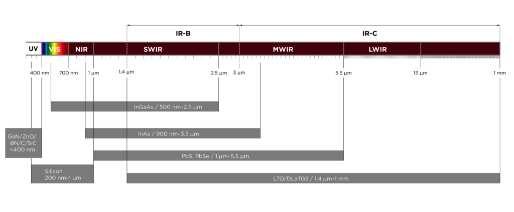
- Spectral range and properties: Spectral range is the wavelength that a photodetector is sensitive to, usually measured in nanometers (nm). The photo below shows some photodetectors that are used to detect signals from long UV to Long Wave Infrared (LWIR) wavelengths. With the long history of photodetector technology, much of the equipment used today may be outdated compared to the latest advances. Development of compounds such as Silicon carbide (SiC), Gallium nitride (GaN), indium gallium arsenide (InGaAs), and other semiconductor materials such as InGaAsSb have recently made high-sensitivity photodetectors. These detectors detect short-wave infrared (SWIR) and mid-wave infrared (MWIR), increasing their power. Organic, graphene-based photodetectors expand opportunities for wearable technology and biomedical applications.
- Quantum Efficiency (QE): Quantum efficiency is the number of charge carriers produced divided by the number of incident photons, usually expressed as a percentage.
- Research (D*): Detection is a normalized factor for the photodetector effect, expressed in Jones (cm·Hz^1/2/W). It combines feedback and noise characteristics. Reactance measures the electrical output per unit of input power, expressed in amperes per watt (A/W) or volts per watt (V/W).
- Noise: Constant attention to the delicate elements is his loud noise, which is a combination of shots and Johnson’s sound of the detective often comes from the current darkness of the detective. Noise Equivalent Power (NEP) is the amount of optical power required to produce a signal equivalent to the noise level of a photodetector, usually measured in watts per root hertz (W/√Hz).
- Device configuration: The structure of the photodetector, including the active area, the thickness of the device and the structure of each layer affect its efficiency, capacity and response time. High-resolution photonics combining special epitaxial layers, such as heterostructures and quantum wells, can improve performance. Pixel design for image applications is very important. Higher pixel density can improve resolution, while larger pixels can improve clarity.
- Speed and response time: Response time is the time it takes for a photodetector to respond to an optical signal, usually measured in nanoseconds (ns) or picoseconds (ps). This affects the detection of photodetectors. Innovations in materials with high electron mobility have reduced the potential, increasing the bandwidth (Hz) of photodetectors.
- Relationship: Close cooperation with end users and industry partners helps to create photodetectors that meet the exact needs of different applications. The hybrid combination of photodetectors and other materials, such as recognition systems, leads to efficient and scalable treatments, increasing efficiency and expanding their range of applications.
- Reliability, durability and strength: Developing photodetectors that can withstand extreme conditions, such as high temperatures, operating pressures and radiation, has increased their use in military, aerospace and industrial applications. This continues with temperature control and packaging. Advances in coating and packaging techniques have shown improved photodetector reliability.
- Cost and equipment: Costs and resources affect all decisions and the potential for investment in photodetector technology is growing. Photonic integrated circuits allow for compact, high-performance systems that are cost-effective. Advances in nanofabrication have allowed the creation of smaller, more efficient photodetectors. Making the photodetector compatible with other advanced semiconductor manufacturing process technologies such as complementary metal-oxide-semiconductor (CMOS) enables the production of low-cost, high-performance sensors.
Photodetector engineers can resolve high-profile issues and the best way forward for success, scalability and future growth by having these conversations on the front end. It is important to comply with standards and certifications quickly, especially for the consumer, automotive, aerospace, defense and medical industries.
Photodetector technology adds and transforms many applications
Today, photodetector technology is an important component supporting countless technologies, including gas sensors, motion sensors and consumer electronics. In communications, it enables high-speed data transmission in fiber optic networks. In aviation and security, they are used for identification and range finding; in R&D, there are many applications of spectroscopy. Their 3D scanning applications are important in building design, construction, autonomous vehicles and industrial control. Photographers also conduct environmental monitoring to identify pollutants and monitor environmental changes. Photoreceptors are also important in medical imaging and are used in devices such as CT scanners and MRI machines for accurate imaging and remote patient monitoring technology.
Photodetector evolution comes with growth challenges
Addressing the company’s pain points often starts with the position of engineers in organizations and the information they need to solve and mitigate challenges. The photonics industry is small, requiring frequent collaboration skills within and across disciplines. Having a dedicated foundation for photographers may not be good for money. Therefore, cooperation is very important for meeting the demands of development. Universities and research institutions stand at the forefront of evolution.
System integration presents another challenge, given the unique applications and need for collaboration within photonics technology. This requires a clear understanding of the product, environment and objectives that are critical to custom, application-specific development.
Designing size, weight, power and cost (SWaP-C) is the most important factor for the design and development of photodetector technology. Investing in dedicated resources is critical to future-proofing plans for growth and innovation as it provides a competitive edge for members in almost any industry.
The future of photodetector technology is bright
Growth and innovation in the application of photodetector technology will continue over time. As this technology becomes more ubiquitous, its success is demonstrated by the small number of people who see the impact in their daily lives. The seamless integration of photodetectors into various applications is a testament to their efficiency and effectiveness. Knowing what to expect is essential to taking advantage of the opportunities in this next generation of innovation. Advances in materials, quantum photonics, integration of AI and sustainable technologies promise to improve performance, efficiency and cost-effectiveness, innovation in autonomous systems, security, medical research, environmental monitoring, consumer electronics and others. As organizations continue to develop and integrate these technologies, there is no denying the full potential for photodetectors to solve complex global challenges and improve daily life. The future holds exciting opportunities, and these advancements are not integrated into the form of our daily experience.
#photodetector #technology #changing #industry #Engineering.com